| Tikalon Blog is now in archive mode.
An easily printed and saved version of this article, and a link
to a directory of all articles, can be found below: |
|
This article |
| Directory of all articles |
Nano Memory
September 30, 2010
I was an undergraduate student of physics in the late 1960s. One controversy that I remember from that period was the publication of the "Ovonic Effect" paper in
Physical Review Letters.[1] The Ovonic effect, named after its discoverer,
Stanford R. Ovshinsky, is the reversible transition between
conductive and
resistive states of some materials caused by application of a voltage. The effect was real, and possibly important because of the rapid switching speed, but there were some problems. The mechanism wasn't exactly understood at the time, and Ovshinsky wasn't a physicist; in fact, he is best characterized as an inventor. Physical Review Letters (PRL) is the preeminent journal for rapid publication of novel discoveries in physics, and the percentage of accepted papers is small (less than 40%). Many submitted papers are referred to other journals. Since Ovshinsky wasn't a member of the physics elite, the cards were stacked against him from the start. Fortunately, a few practicing physicists made the case that his paper should be published in PRL. As history would show, this effect has led to the exciting memory technology known as
phase change memory.
The materials Ovshinsky investigated were
chalcogenide glasses, specifically
selenides and
tellurides. One such material is Ge
2Sb
2Te
5. Chalcogenide glasses have a highly resistive
amorphous state and a low resistivity
crystalline state. Application of proper voltages allows switching between these states and allows memory operation. The switching occurs in a few tens of nanoseconds, but research is in progress to reduce this swiching time.
A recent article in
IEEE Spectrum reviews progress in a similar type of memory called
resistive random-access memory (RRAM).[2] Just as in phase-change materials, RRAM materials transform between insulating and conductive states. These are not phase changes. Instead, application of a voltage causes a filamentary conductive path to form in the material, typically from the migration of atoms to defects, such as lattice
vacancies,
dislocations and
grain boundaries. The effect is reversible, and it's fast. One such RRAM material is the
perovskite, Pr
0.7Ca
0.3MnO
3. RRAM requires lower power for operation than phase-change memory, so it's a favored technology for mobile devices.
New memory technologies are becoming important, since conventional memory cells, in which the logic state is stored as a charge on a
capacitor, have reached their limits as to how much they can be reduced in size. Also,we shouldn't forget the problem of soft memory errors for this type of memory device, as I summarized in a
previous article (Fleeting Memory, September 28, 2006).
Cosmic rays strike the
Earth quite often. When they hit a semiconductor chip, they can form millions of
electron-hole pairs that can change the charge state of a memory capacitor and cause a transient memory error. Phase change memory has no capacitor, so it's immune to this type of error. RRAM is also immune.
The size of a memory cell can be considerably reduced if the capacitor and its associated
field effect transistors are not required. The simplest architecture is a crossbar array in which tiny blobs of a RRAM material are contained between orthogonal conductors. Each particular blob can be accessed via a unique (x,y) address (see figure, for which elements "14" and "18" are the crossbar conductors, and "42" is the memory material). Reading a memory cell is easy. All that's required is a
current source and a
comparator that distinguishes a high voltage drop (the insulating state) from a low voltage drop (the conductive state). Writing is done via applied voltages that put the RRAM material into the proper regime for the desired action. RRAM crossbar memory arrays with features less than 20 nanometers are expected by 2015.[2] Certain RRAM materials are optimized for speed, and others for data retention.
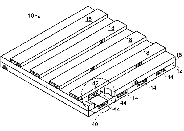
RRAM Crossbar Memory; Fig. 1 of US patent 6,531,371.
Although phase-change memories might be too power hungry for mobile devices, research continues for other applications. Scientists at
Lawrence Berkeley National Laboratory and the
University of California at Berkeley have discovered a new class of phase-change materials called binary eutectic-alloy nanostructures (BEANs), which are
nanocrystals of
alloys of a
metal and a
semiconductor.[3-4] In their experiments, they used GeSn nanoparticles embedded in
silica. GeSn is a
eutectic alloy and a prototypical phase-change material that has stable crystalline and amorphous states at room temperature. Switching times of just nanoseconds were achieved by the Berkeley team, and this material can be switched electrically or optically. Embedding nanoparticles of the alloy in a matrix allows the rapid cooling that's required to stabilize the amorphous phase. Moderate heating, followed by a slower ramp to room temperature, produces the crystalline state. More work is required to characterize the robustness of the Berkeley material after repeated cycling.
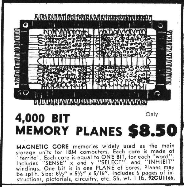
Ad for surplus ferrite core memory planes, circa 1970 (from Poly Paks catalog No. 192; scan by the author). We've come a long way in memory technology.
References:
- Stanford R. Ovshinsky, "Reversible Electrical Switching Phenomena in Disordered Structures," Physical Review Letters, vol. 21, no. 20 (1968), pp. 1450-1453.
- David Lammers, "Resistive RAM Gains Ground," IEEE Spectrum (September 2010).
- Lynn Yarris, "Magical BEANs: New Nano-sized Particles Could Provide Mega-sized Data Storage," Lawrence Berkeley National Laboratory Press Release, September 16, 2010.
- S. J. Shin, J. Guzman, C.-W. Yuan, Christopher Y. Liao, Cosima N. Boswell-Koller, P. R. Stone, O. D. Dubon, A. M. Minor, Masashi Watanabe, Jeffrey W. Beeman, K. M. Yu, J. W. Ager, III, D. C. Chrzan and E. E. Haller, "Embedded Binary Eutectic Alloy Nanostructures: A New Class of Phase Change Materials," Nano Letters, vol. 10, no. 8 (July 16, 2010), pp. 2794-2798.
- Web page of the Daryl C. Chrzan Research Group at the University of California, Berkeley
Permanent Link to this article
Linked Keywords: Physical Review Letters; Stanford R. Ovshinsky; conductive; resistive; phase change memory; chalcogenide glasses; selenides; tellurides; amorphous; crystalline; IEEE Spectrum; resistive random-access memory; vacancies; dislocations; grain boundaries; perovskite; capacitor; soft memory errors; cosmic rays; Earth; electron-hole pairs; field effect transistors; current source; comparator; US patent 6,531,371; Lawrence Berkeley National Laboratory; University of California at Berkeley; nanocrystals; alloys; metal; semiconductor; silica; eutectic; ferrite core memory.