| Tikalon Blog is now in archive mode.
An easily printed and saved version of this article, and a link
to a directory of all articles, can be found below: |
|
This article |
| Directory of all articles |
Gallium Nitride Crystals
July 29, 2010
As my
curriculum vitae indicates, I was involved in
crystal growth for many years. Crystal growth is truly interdisciplinary, since crystal growers do a little physics, a little chemistry, a little engineering, and a lot of praying. The first successfully mass-produced crystal was
quartz, since quartz crystals are used in electronic oscillators. The
hydrothermal synthesis of quartz, a technique that used high pressure, high temperature reactors, was invented by Charles B. Sawyer of Cleveland, Ohio. The hydrothermal synthesis technique is an analog of the way that nature produces quartz crystals.
The preeminent synthetic crystal is
silicon, produced for
integrated circuit fabrication. Silicon crystals are grown by the
Czochralski process, named after its inventor,
Jan Czochralski. Czochralski, a Polish chemist, developed this process in 1916 in an attempt to produce metal wires without the usual drawing process. In his process, you dip a seed crystal into a crucible of molten material slightly above its melting point and slowly withdraw a large crystal mass that attaches itself to the seed.
Gordon Teal of
Bell Labs adapted the process to the growth of the
germanium crystals used for the first transistors. I was privileged to work for a time with
Ernie Buehler, who was a member of the team that produced the germanium for the first transistor. Ernie was a prime example that you don't need a PhD to do good science.
Not very much later, the Czochralski process was adapted to the growth of crystals of
silicon, which has some advantages over germanium in transistors and integrated circuits. There have been a few latecomers to the game, including
gallium arsenide and
indium phosphide, which are both used for light-emitting diodes and extremely high frequency circuits; but silicon still reigns supreme. However, blue, violet and ultraviolet light-emitting diodes and lasers can't be made from silicon.
Shuji Nakamura developed a
technique for production of such devices on
gallium nitride at
Nichia Corporation, and gallium nitride has become an important electronic crystal. Blu-ray disc players use a gallium nitride violet laser diode, and gallium nitride is also a useful material for power electronics.
Growth of gallium nitride crystals is not as easy as the growth of silicon. Gallium nitride is only molten at 2225
oC, and at that temperature a pressure of nitrogen of 64,000 atmospheres must be maintained to keep the material from decomposing. Such conditions would be impossible to produce in a large volume apparatus in a laboratory. One early technique for making gallium nitride substrates was
heteroepitaxy, which is the process of putting a thin layer of gallium nitride onto another type of wafer, typically
sapphire. The gallium nitride is deposited by
hydrogen reduction of gallium and nitrogen gaseous
precursor compounds at a hot substrate. If the epitaxial layer is grown thick enough, the sapphire substrate can be removed and reused. A fundamental disadvantage of this process is that the gallium nitride layer has quite a few defects, since the spacing of atoms of its crystal lattice doesn't precisely match that of the substrate.
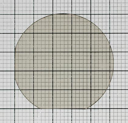
A GaN wafer (from Ammono web site).
Luckily, the same technique used for production of quartz crystals can be used to make gallium nitride, and a Polish company,
Ammono, in
Warsaw, has been working for the last two decades perfecting this approach.[1-2] According to their web site, it's taken more than 2,200 experiments for them to reach the point that they are able to routinely produce high quality gallium nitride substrates two inches in size; and they are striving for 100mm wafers that will fit the mass production machines of device manufacturers. In adapting the quartz process to gallium nitride, Ammono uses reactors that operate at 550
o C and 5000 atmospheres pressure with an ammonia solvent (thus the name, "Ammono"). They found that it was essential to keep any traces of oxygen from the reactors. A pinch of alkali metals helps to keep the pressures low, since nitrogen is dissolved readily in them. A similar technique has been used in batteries, where hydrogen-absorbing materials are used.
Ammono has had consistent financial support from Nichia, and it hopes to produce two-inch wafers by year's end, three-inch in 2013, and four-inch in 2015. Their business plan is being driven by the violet laser market, which stands at about $100 million, today, with a double digit compound annual growth rate. Ammono estimates a price of $1,000 per two-inch wafer with subsequent price reductions. For comparison, four-inch gallium arsenide wafers presently sell for $200.
References:
- Virgil E. Bottom, "A History Of The Quartz Crystal Industry In The USA," Proceedings of the 35th Annual Frequency Control Symposium (1981), pp. 3-12.
- Ammono Home Page.
- Richard Stevenson, "The World's Best Gallium Nitride," IEEE Spectrum, July 2010.
- R. Dwilinski, R. Doradzinski, J. Garczynski, L.P. Sierzputowski, A. Puchalski, Y. Kanbara, K. Yagi, H. Minakuchi and H. Hayashi, "Excellent crystallinity of truly bulk ammonothermal GaN," Journal of Crystal Growth, vol. 310 (2008), pp. 3911.
- R. Dwilinski, R. Doradzinski, J. Garczynski, L.P. Sierzputowski, A. Puchalski, Y. Kanbara, K. Yagi, H. Minakuchi and H. Hayashi, "Bulk ammonothermal GaN," Journal of Crystal Growth, vol. 311 (2009), pp. 3015-3018.
- R. Dwilinski, R. Doradzinski, J. Garczynski, L.P. Sierzputowski, M. Rudzinski and M. Zajac,"Homoepitaxy on bulk ammonothermal GaN," Journal of Crystal Growth, vol. 311 (2009), pp. 3058-3062.
Permanent Link to this article