Calvin Quate (1923-2019)
October 14, 2019
Children are
curious, and their curiosity includes the need to discover how the
artifacts in their
environment work. Children will sometimes take things apart to seek out their inner
mechanism. This effort was much more rewarding in
my generation, when opening a
toy would reveal simple things like
gears and
springs; or, a
battery,
switch,
lights, and a
motor. Today, most toys are stuffed with
inscrutable integrated circuits, so the adventure is not as rewarding.
Throughout
history,
humans have examined their environment as closely as they could to discover why some items, such as
plants, are different from other items, such as
rocks. We were limited in such studies by the
visual acuity of the unaided
eye, which is about an
arc minute in the best of cases. If you've ever wondered why
ancient astronomy was so advanced despite the lack of
telescopes, there are about 40,000
square degrees in a
sphere, and more than 50 million
square minutes in a
hemisphere.
Going from very large and distant objects to very close and small objects, the unaided eye can see specks as small as a tenth
millimeter (100
micrometers).
Eukaryotic cells range in size up to about 100 micrometers. A human
red blood cell has a size of about 7.5 micrometers, while cells of
cork can be as large as about 50 micrometers. It's understandable that
cells were discovered only after the
microscope was invented.
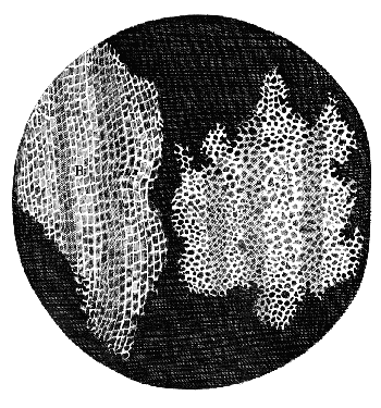
A 1665 engraving of cork cells from Micrographia by Robert Hooke (1635-1703), 1665.
Robert Hooke was the first to observe cells, which he named after the small rooms, called cella, in which monks lived. The cork cells that he observed were empty cell walls devoid of their internal cell components.
As Hooke wrote in the Micrographia, "...Our microscope informs us that the substance of Cork is altogether fill'd with Air, and that the Air is perfectly enclosed in little Boxes or Cells..."[1]
(Via Wikimedia Commons)
While the
optical microscope allowed us to image things with size about the
wavelength of
light, 500
nanometers, there's a lot of detail in
nature below that limit. Early in the
20th century, it was realized that it was possible to do
microscopy with electrons with better detail, since the
de Broglie wavelength of electrons is many
orders of magnitude smaller than the wavelength of light. The first such
electron microscope was the
transmission electron microscope that images by the
attenuation of
electron beam intensity through a thin
specimen. This concept was enabled by the use of
magnetic fields acting as
electron lenses to
focus and
magnify the electron beam.
While the transmission electron microscope offered very high
resolution, sample preparation was tedious. Furthermore, many
research investigations didn't need such high magnification, but they did need a wide
field of view. The
scanning electron microscope (SEM) filled the gap between optical microscopy and transmission electron microscopy with an
instrument that scanned a specimen in a
raster pattern, as is done in a
cathode ray tube, and imaging by detection of
secondary electrons generated by the raster electrons, or by the
backscattered raster electrons. SEM images have the
three-dimensional appearance of their optical microscopy cousins, so they provide
topographic information for things such as integrated circuits.
Older readers might remember their
mother's admonition to sit well away from the
television screen because of
X-rays. While
safety standards were established to preclude X-ray generation in cathode ray tube televisions, it's also true that the electron beam in an SEM will excite
characteristic X-rays of the
elements in a specimen so that the
material composition can be identified using
energy-dispersive X-ray spectroscopy (EDAX) or
wavelength dispersive X-ray spectroscopy (WDXS).
Environmental scanning electron microscopes allow imaging of
biological specimens, which is quite a trick, since electrons need to travel in a
vacuum and biological specimens contain
water with a high
vapor pressure.
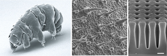
Animal, vegetable, or mineral>.(Left image, an SEM image of Milnesium tardigradum from Comparative proteome analysis of Milnesium tardigradum in early embryonic state versus adults in active and anhydrobiotic state by Elham Schokraie, Uwe Warnken, Agnes Hotz-Wagenblatt, Markus A. Grohme, Steffen Hengherr, Frank Förster, Ralph O. Schill, Marcus Frohme, Thomas Dandekar, and Martina Schnölzer, PLoS ONE, vol. 7, no. 9 (September 27, 2012), Article No. e45682, doi:10.1371/journal.pone.0045682; center image, an SEM image of tricomes and stomates on a Nicotiana alata upper leaf surface by Louisa Howard of Dartmouth University; and, right image, and SEM image of a nanohole array etched in amorphous silicon, all from Wikimedia Commons. Click for larger image.)
While it's very easy to generate electrons having a
de Broglie wavelength of the order of
atomic size, imaging by electrons depends on how well you can focus an electron beam, so atomic imaging by electrons is difficult. In
high-resolution transmission electron microscopy (HRTEM), both the
phase and
amplitude of the electron wave are used to resolve individual atoms. Transmission electron microscope are huge, complex, and expensive instruments, so there was always a need for an easier way to image at the atomic scale, and the first successful attempt at this was the
scanning tunneling microscope (STM).
The scanning tunneling microscope was
invented by
Gerd Binnig and
Heinrich Rohrer who were working at the
IBM Research-Zurich research laboratory in the
1980s.[2] They were awarded the 1986
Nobel Prize in Physics for this invention, which was facilitated by modern
electronic technology. The imaging process of an STM is extremely simple. A sharp
metal tip is scanned across a
conducting surface, and it's held just out of contact range by monitoring a
voltage created by
quantum mechanical tunneling and adjusting the tip position to maintain a fixed tunneling
current. A resolution of 10
picometers, sufficient to image atoms, is possible with an STM; but, just as importantly, no vacuum is required.
Shortly after the demonstration of the STM, Bennig invented the
atomic force microscope (AFM),[3] which he demonstrated along with
Calvin Quate and
Christoph Gerber in 1986.[4-6] While an AFM scans a sharp
probe tip across the specimen surface, just like an STM, what's measured is not the tunneling current but a
force on the
cantilever on which the probe tip is attached. As a consequence, an AFM can image a non-conductive surface while an STM cannot. The STM is strictly a non-contact technique, while the AFM probe tip can gently contact the specimen surface or operate in a non-contact mode. Imaging is done by measurement of the force on the cantilever that changes as the topography or attraction of the probe tip to the surface changes, as by the
van der Waals force or other forces.
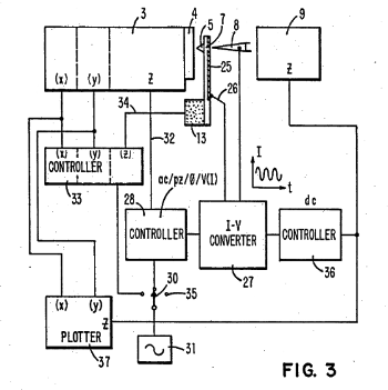
Figure three from US patent no. 4,724,318, "Atomic force microscope and method for imaging surfaces with atomic resolution," by Gerd K. Bennig, February 9, 1988.
Electronics has enabled many scientific advances, and the atomic force microscope is a good example.
Aside from creation of a suitable imaging tip, all the magic of an AFM is in its associated electronics.
The probe for the first atomic force microscope was a diamond tip mounted on gold foil cantilever. The gold foil was only 25 micrometers thick and 0.8 millimeters long so it would bend sufficiently under small force.[6]
While the patent shows imaging with an X-Y plotter, modern AFMs use computer imaging techniques.
(Via Google Patents.[3])
Not only is an AFM easier to build, but the imaging force can arise in a number of ways. These include the
mechanical force of surface contact,
chemical bonding and van der Waals forces,
capillarity, and
magnetic attraction. The resolution of an AFM is usually better than that of an STM, so it's more often used. An AFM can have different modes of operation, the simplest being the contact mode. There's a tapping mode in which the probe tip taps the surface at each position, and the non-contact mode in which the probe tip is
oscillated very close to the specimen surface, and the change in attraction force is inferred by a change in cantilever amplitude or
frequency.
Calvin Quate, one of the developers of the atomic force microscope, died on July 6, 2019, at the age of 95.[7-9]
At his death, Quate was the Leland T. Edwards
Professor of
Engineering,
Emeritus, and a professor of
applied physics at
Stanford University (Stanford, California).[8] Throughout his life, he was an avid
outdoorsman who liked to
ski,
hike,
jog,
kayak and
windsurf.[9] This love of the outdoors may have arisen from his
childhood in
Baker, Nevada, where he rode
horses,
tended sheep, and explored nearby
mountains.[7-8] His
family relocated to
Salt Lake City, Utah, in 1934, where he got his
bachelor's degree in
electrical engineering at the
University of Utah in 1944.[8]
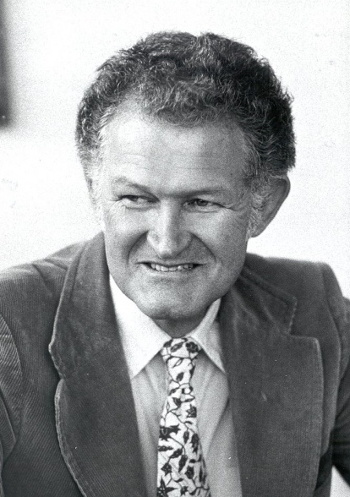
Calvin Quate (1923-2019).
(IEEE History Center image, used with permission.[9])
Upon
graduation from the University of Utah, Quate became part of the
Manhattan Project at
Oak Ridge National Laboratory,
Tennessee.[8] After Oak Ridge, he became a
graduate student at Stanford University and earned his
Ph.D. in electrical engineering in 1950.[7] He joined
Bell Laboratories,
Murray Hill, New Jersey, for
microwave research in 1949, and he rose to become
Associate Director of Electronics Research.[8-9] Quate joined
Sandia Corporation in
Albuquerque, New Mexico, in 1959, where he quickly became
Vice President and Director of Research.[9]
In 1961, Quate joined Stanford University as Professor of
Applied Physics and Electrical Engineering. At Stanford, he was Chairman of the Applied Physics Department (1969-1972 and 1978-1981), Acting Chairman of the Electrical Engineering Department (1986-1988), and
Associate Dean in the
School of Humanities and Science (1972-1974).[8-9] At Stanford, Quate realized that the wavelength of
gigahertz acoustic waves in water can be smaller than that of light.[7] This
intuition, and the development of acoustic lenses capable of focusing sound to a sub-micrometer spot size, led to the invention of the
scanning acoustic microscope in 1978.[7]
The acoustic microscope allowed sharp
contrast imaging of things that were not easily seen optically, including sub-surface structures in integrated circuits.[9] The acoustic waves were delicate enough to measure the
mechanical properties of living cells.[8] Quate was recognized by
R&D Magazine as Scientist of the Year for 1995 for his invention of the acoustic microscope and his work on atomic force microscopy.[8] In 1995, these two instruments constituted a $100 million instrument industry.[8]
Quate's Stanford colleagues remember him as a quiet and
affable person who offered an
opinion only when asked. As
Robert Byer of the Department of Applied Physics recalled, "He earned respect with very few words. Everyone listened to what Cal Quate had to say."[8]
James Gibbons, former dean of the Stanford School of Engineering said that "His position on most matters of
academic administration can be stated in two short sentences: 'Do we need to do this?' or 'I'll do it.' I felt honored to know him and I will miss him greatly."[8]
Quate was a
Fellow of the
IEEE, and a member of the
National Academy of Engineering and the
National Academy of Sciences.[9] He was awarded the Rank Prize for
opto-electronics from the
Royal Society of London for his work on the scanning acoustic microscope in 1982, and the
IEEE Medal of Honor in 1988 for the invention and development of the scanning acoustic microscope.[8-9] He became a member of the Royal Society in 1995, and he was a fellow of the
Norwegian Academy of Science and Letters.[8]
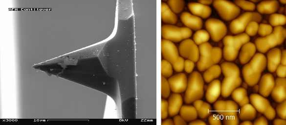
Left image, a probe tip for an atomic force microscope. Right image, an AFM micrograph of a magnetron sputtered tin layer by Piret Pikma. (Both images from Wikimedia Commons. Click for larger image.)
References:
- Robert Hooke, "Micrographia: or, Some physiological descriptions of minute bodies made by magnifying glasses," (J. Martyn & J. Allestry, London, 1665), p. 112f.
- G. Binnig, H. Rohrer, Ch. Gerber, and E. Weibel, "Surface Studies by Scanning Tunneling Microscopy," Phys. Rev. Lett., vol. 49, no. 1 (July 5, 1982), pp. 57ff., DOI:https://doi.org/10.1103/PhysRevLett.49.57. This is an open access article with a PDF file here.
- Gerd K. Bennig, "Atomic force microscope and method for imaging surfaces with atomic resolution," US Patent No. 4,724,318, February 9, 1988 (Via Google Patents).
- G. Binnig, C. F. Quate, and Ch. Gerber, "Atomic Force Microscope," Phys. Rev. Lett., vol. 56, no. 9 (3 March 3, 1986), pp. 930ff., DOI:https://doi.org/10.1103/PhysRevLett.56.930 This is an open access article with a PDF file here.
- Scanning Probe Microscopy: From Sublime to Ubiquitous, Phys. Rev. Lett. vol. 90, Article No. 115505, 2003.
- David Lindley, "Focus: Landmarks—Atomic Force Microscope Makes Angstrom-Scale Images," Physics, vol. 5, no. 106, September 21, 2012
- Daniel Rugar and Franz Giessibl, "Calvin F. Quate (1923–2019)," Science, vol. 365, no. 6455 (August 23 2019), pp. 760, DOI: 10.1126/science.aay9386.
- Andrew Myers, "Calvin F. Quate, inventor of advanced microscopes, dies at 95," Stanford University Press Release, July 10, 2019.
- Calvin F. Quate - Biography, Engineering and Technology History Wiki, IEEE History Center.
Linked Keywords: Child; children; curiosity; curious; cultural artifact; biophysical environment; mechanism (engineering); baby boomer; my generation; toy; gear; spring (device); battery; electric switch; electric light; electric motor; inscrutable; integrated circuit; history; human; plant; rock; visual acuity; eye; arc minute; ancient astronomy; telescope; square degree; sphere; square minute; hemisphere; millimeter; micrometer; Eukaryote; Eukaryotic; cell (biology); red blood cell; cork (material); discovery of cells; microscope; engraving; Micrographia; Robert Hooke (1635-1703); monk; cell wall; Wikimedia Commons; optical microscope; wavelength; light; nanometer; nature; 20th century; electron microscope; matter wave; de Broglie wavelength; order of magnitude; transmission electron microscope; attenuation; cathode ray; electron beam; intensity (physics(; sample (material); specimen; magnetic field; electron lens; focus (optics); magnification; magnify; angular resolution; research; field of view; scanning electron microscope; scientific instrument; raster scan; cathode ray tube; secondary emission; secondary electron; backscatter; three-dimensional; topography; topographic; mother; admonition; television set; television screen; X-rays; radiation protection; safety standard; chemical element; material; composition; energy-dispersive X-ray spectroscopy (EDAX); wavelength dispersive X-ray spectroscopy (WDXS); Environmental scanning electron microscope; biology; biological; vacuum; water; vapor pressure; Milnesium tardigradum; leaf epidermis; nanohole array; atomic radius; atomic size; high-resolution transmission electron microscopy (HRTEM); phase (waves); amplitude; scanning tunneling microscope (STM); invention; invented; Gerd Binnig; Heinrich Rohrer; IBM Research-Zurich research laboratory; 1980s; Nobel Prize in Physics; electronic technology; metal; electrical conductor; surface; voltage; quantum mechanical tunneling; picometer; atomic force microscope (AFM); Calvin Quate (1923-2019); Christoph Gerber; probe tip; force; cantilever; van der Waals force; patent; electronics; science; scientific; diamond; gold; foil; micrometer; millimeter; deflection (engineering); bend; force; X-Y plotter; computer; Google Patents; classical mechanics; mechanical; chemical bond; chemical bonding; capillary action; capillarity; magnetic field; magnetic; oscillation; oscillate; frequency; professor; engineering; Emeritus; applied physics; Stanford University (Stanford, California); outdoor enthusiast; outdoorsman; skiing; hiking; jogging; kayaking; windsurfing; childhood; Baker, Nevada; horse; shepherd; sheep; mountain; family; Salt Lake City, Utah; bachelor's degree; electrical engineering; University of Utah; IEEE History Center; graduation; Manhattan Project; Oak Ridge National Laboratory; Tennessee; postgraduate education; graduate student; Doctor of Philosophy; Ph.D.; Bell Labs; Bell Laboratories; Murray Hill, New Jersey; microwave; Associate Director; Sandia National Laboratories; Sandia Corporation; Albuquerque, New Mexico; Vice President; Applied Physics and Electrical Engineering; Associate Dean; School of Humanities and Science; gigahertz; acoustic wave; intuition (philosophy); scanning acoustic microscope; contrast; mechanical properties; R&D Magazine; affable; opinion; Robert Byer; James Gibbons; academia; academic; administration; Fellow; Institute of Electrical and Electronics Engineers; IEEE; National Academy of Engineering; National Academy of Sciences; optoelectronics; Royal Society of London; IEEE Medal of Honor; Norwegian Academy of Science and Letters; micrograph; sputter deposition; magnetron sputtered; tin; Gerd K. Bennig, "Atomic force microscope and method for imaging surfaces with atomic resolution," US Patent No. 4,724,318, February 9, 1988.