Quilting Semiconductors
September 26, 2014
Semiconductor electronics is based on the principle that
electrons behave differently in different
materials. Sometimes the difference is just small
concentrations of different
impurities in the same material. One example is
silicon, for which small additions of an
element with excess
electrons, called a
donor, will make an
N-type material, while adding an element deficient in electrons, called an
acceptor, will make a
P-type material.
For silicon,
arsenic is a typical donor, having five
valence electrons to silicon's four, while
boron, with three valence electrons, is a typical acceptor. Joining N- and P-type materials results in a
diode that allows
current to flow in one direction, only. Because of an
energy difference seen by electrons in these two materials, electrons will flow from the
cathode (N-type) to the
anode (P-type), but not in the reverse direction.
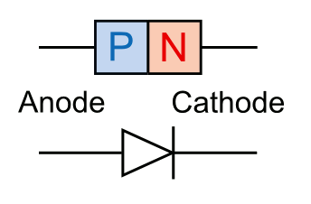
Semiconductor diode P-N junction and symbol.
(Illustration by the author, rendered using Inkscape.)
When there are different materials on opposite sides of the junction, the structure is called a
heterojunction. Heterojunctions are useful in the fabrication of
semiconductor lasers, high speed
transistors, and high speed
optical detectors. Just as in the standard junction case, these heterojunctions are made by putting one material layer over another. Now, a team of
scientists from the
University of Washington (Seattle, Washington), the
University of Warwick (Coventry, UK), and the
University of Hong Kong (Hong Kong, China) have made side-by-side junctions of
atomically thin materials; that is, they made
lateral heterostructures. They made a semiconductor quilt.[1-2]
I've always enjoyed looking at
quilts. Quilts had a
utilitarian purpose in the past, since
sewing together discarded
clothing remnants into a
bed covering was a useful task. Today, they're more likely to be found on a
wall as
decoration than on a
bed. The lateral heterojunctions were a quilt of
molybdenum diselenide, MoSe
2, and
tungsten diselenide, WSe
2.[1-2]
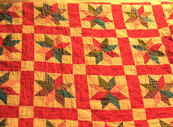
We had a quilt like this in our house.
It's apparently a traditional style.
(Photograph by Brooke Raymond, via Wikimedia Commons.)
Molybdenum diselenide and tungsten diselenide are similar to
graphene in that they produce
monolayers with strong in-plane
bonding, but weak layer-to-layer bonding by
van der Waals forces, only. Like graphene, these materials appear to have some very useful electronic properties
Tungsten diselenide, in particular, seems to be more useful than graphene, as a number of recent
journal articles illustrate.[3-8] I wrote about tungsten diselenide in a
recent article (Light-Emitting Diodes of Tungsten Diselenide, March 17, 2014). Unlike graphene, these two selenides are
direct bandgap semiconductors, which means that they will function as
light emitters.
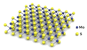
A layer of molybdenum disulfide, a close cousin to molybdenum diselenide and tungsten diselenide.
(Via arXiv Preprint Server))
These lateral heterojunctions could be
grown without
lattice defects because the two selenides have the same
crystal structure.[1-2] Says senior
author of the study,
Xiaodong Xu, an
assistant professor of
physics, and also
materials science and engineering, at the University of Washington,
"Heterojunctions are fundamental elements of electronic and photonic devices... Our experimental demonstration of such junctions between two-dimensional materials should enable new kinds of transistors, LEDs, nanolasers, and solar cells to be developed for highly integrated electronic and optical circuits within a single atomic plane."[2]
The process for
fabrication was not difficult.
Hydrogen transport
chemical vapor deposition was done at 900
°C, first a partial layer of one selenide was produced on a
substrate. This appeared as small triangular islands of two-dimensional crystal. Then the same was done for the other selenide, whose atoms filled the voids between these patches to produce the heterojunction quilt.[2]
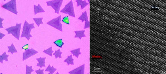
Right, an optical micrograph of a lateral heterostructure layer in which the two selenides are distinguished by color. Left, a high-resolution scanning transmission electron microscopy (STEM) image showing a seam with atomic precision. (Right image by the University of Washington. Left image by the University of Warwick.)[2]
As explained by
Sanfeng Wu, a
Ph.D. candidate in physics at the University of Washington and one of the lead authors,
"This is a scalable technique... Because the materials have different properties, they evaporate and separate at different times automatically. The second material forms around the first triangle that just previously formed. That's why these lattices are so beautifully connected."[2]
The heterojunction growth, itself, took about five minutes, with an additional two hours for heating and cooling time.[2] Using
optical microscopy, the lateral heterojunctions showed enhanced
photoluminescence, which demonstrates their
optoelectronic potential.[1-2]
Atomically resolved scanning transmission electron microscopy at the University of Warwick showed that the two selenides join together in an undistorted
hexagonal lattice with a graduation of
molybdenum and
tungsten atoms across the boundary region.[1-2]
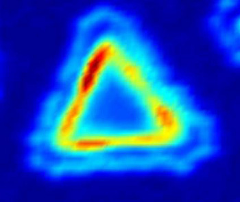
Photoluminescence emission intensity map of a molybdenum diselenide-tungsten diselenide lateral heterostructure.
The photoluminescence illustrates the potential optoelectronic applications of the material.
(University of Washington image.)[2]
Such lateral heterojunctions could enable in-plane transistors and diodes, all of which could be integrated within one atomically thin layer.[1-2]
Funding for this research came from the
U.S. Department of Energy, the
Clean Energy Institute at the University of Washington, the
Research Grant Council of Hong Kong, the
University Grants Committee of Hong Kong, the
Croucher Foundation, the
Science City Research Alliance and the
Higher Education Funding Council for England's Strategic Development Fund.[2]
References:
- Chunming Huang, Sanfeng Wu, Ana M. Sanchez, Jonathan J. P. Peters, Richard Beanland, Jason S. Ross, Pasqual Rivera, Wang Yao, David H. Cobden , and Xiaodong Xu, "Lateral heterojunctions within monolayer MoSe2–WSe2 semiconductors," Nature Materials, Article no. 4064 (August 24, 2014), doi:10.1038/nmat4064.
- Michelle Ma, "Scientists craft atomically seamless, thinnest-possible semiconductor junctions," University of Washington Press Release, August 26, 201.
- Jason S. Ross, Philip Klement, Aaron M. Jones, Nirmal J. Ghimire, Jiaqiang Yan, D. G. Mandrus, Takashi Taniguchi, Kenji Watanabe, Kenji Kitamura, Wang Yao, David H. Cobden and Xiaodong Xu, "Electrically tunable excitonic light-emitting diodes based on monolayer WSe2 p–n junctions," Nature Nanotechnology (March 9, 2014), doi:10.1038/nnano.2014.26.
- Jason S. Ross, Philip Klement, Aaron M. Jones, Nirmal J. Ghimire, Jiaqiang Yan, D. G. Mandrus, Takashi Taniguchi, Kenji Watanabe, Kenji Kitamura, Wang Yao, David H. Cobden and Xiaodong Xu, "Electrically tunable excitonic light-emitting diodes based on monolayer WSe2 p–n junctions," arXiv Preprint Server, March 4, 2014.
- Britton W. H. Baugher, Hugh O. H. Churchill, Yafang Yang and Pablo Jarillo-Herrero, "Optoelectronic devices based on electrically tunable p–n diodes in a monolayer dichalcogenide," Nature Nanotechnology (March 9, 2014), doi:10.1038/nnano.2014.25.
- Andreas Pospischil, Marco M. Furchi and Thomas Mueller, "Solar-energy conversion and light emission in an atomic monolayer p–n diode," Nature Nanotechnology (March 9, 2014), doi:10.1038/nnano.2014.14.
- David L. Chandler, "Two-dimensional material shows promise for optoelectronics," MIT Press Release, March 10, 2014.
- Michelle Ma, "Scientists build thinnest-possible LEDs to be stronger, more energy efficient," University of Washington Press Release, March 10, 2014.
Permanent Link to this article
Linked Keywords: Semiconductor; Solid-state electronics; electron; material; concentration; impurity; silicon; chemical element; donor; N-type; acceptor; P-type; arsenic; valence electron; boron; diode; eectric current; potential energy; energy difference; cathode; anode; Inkscape; heterojunction; laser diode; semiconductor laser; transistors; photodetector; optical detector; scientist; University of Washington (Seattle, Washington); University of Warwick (Coventry, UK); University of Hong Kong (Hong Kong, China); atom; atomically thin; lateral; quilt; utility; utilitarian; sewing; clothing remnant; banket; bed covering; wall; decoration; bed; molybdenum diselenide; tungsten diselenide; Brooke Raymond; Wikimedia Commons; graphene; transition metal dichalcogenide monolayer; chemical bond; van der Waals force; scientific literature; journal article; direct bandgap; light-emitting diode; light emitter; molybdenum disulfide; crystal growth; crystal structure; lattice; crystallographic defect; author; Xiaodong Xu; assistant professor; physics; materials science and engineering; photonics; photonic; experiment; experimental; light-emitting diode; LED; nanolaser; solar cell; integrated circuit; optical; circuit; semiconductor device fabrication; hydrogen; chemical vapor deposition; celsius; °C; wafer; substrate; optical micrograph; scanning transmission electron microscopy; precision; Sanfeng Wu; Doctor of Philosophy; Ph.D.; evaporation; evaporate; optical microscopy; photoluminescence; optoelectronic; atom; atomically resolved; hexagonal lattice; molybdenum; tungsten; photoluminescence emission; intensity; map; Funding of science; U.S. Department of Energy; Clean Energy Institute at the University of Washington; Research Grant Council of Hong Kong; University Grants Committee of Hong Kong; Croucher Foundation; Science City Research Alliance; Higher Education Funding Council for England's Strategic Development Fund.