Light-Emitting Diodes of Tungsten Diselenide
March 17, 2014
Layered
materials have become the darling of our age of
nanotechnology. It's easy to strip away flakes of just a few
atomic layers from some materials. It all started with
graphene, single-layer sheets of
carbon atoms harvested from the
graphite allotrope of carbon by the simple process of sticking a piece of
cellophane tape on a piece of graphite and pulling it off. You can see a demonstration of this process in a
YouTube video.[1]
Since the layers of graphite easily detach and slide against each other, graphite is used as a
lubricant. The
United States Geological Survey estimates that 1,350
metric tons of graphite were used as a lubricant in the
United States in 2012.[2] The
hexagonal polymorph of
boron nitride, composed of
elements flanking carbon in the periodic table, has a structure like graphite, and it's also a good lubricant.
Molybdenum disulfide (molybdenite,
MoS2), is another hexagonal layered material used as a lubricant (see figure). I wrote about molybdenum disulfide in a
previous article (Molybdenum Disulfide Circuitry, December 9, 2011). The lubricity arises from the weak
atomic forces binding the adjacent atomic planes of
sulfur.
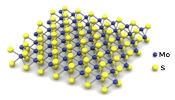
A layer of molybdenum disulfide (molybdenite, MoS2).[3]
(Via arXiv Preprint Server))
Tungsten diselenide (WSe
2), a compound formed from layers of
tungsten and
selenium, has an hexagonal crystal structure like that of molybdenum disulfide. As early as 1985, WSe
2 was shown to be an effective
photovoltaic material with 14%
efficiency under
simulated solar radiation, albeit with a
polyiodide liquid junction.[4] This presaged some recent work on making
junction diodes of tungsten diselenide, and
light emitting diodes as well.
Experiments on junction diodes of tungsten diselenide were reported in a trio of papers in a recent issue of
Nature Nanotechnology.[5,8-9] One of these was authored by a group at the
Massachusetts Institute of Technology.[8] Another at the
Vienna University of Technology (Vienna, Austria).[9] The third was by a large international team of scientists from the
University of Washington (Seattle, Washington), the
Justus Liebig University (Giessen, Germany), the
University of Tennessee (Knoxville, Tennessee),
Oak Ridge National Laboratory (Oak Ridge, Tennessee), the
National Institute for Materials Science (Tsukuba, Japan), and the
University of Hong Kong (Hong Kong, China).[5] It appears that in this
research, as in other examples, the research teams get larger as the materials get smaller.
The most interesting feature of the reported tungsten diselenide devices is the way that the junctions are formed. The
n-type and
p-type materials are formed by
electrically biasing the thin WSe
2 sheets with
metal electrodes. A thin boron nitride layer is used as an isolating
dielectric between the biasing metal and WSe
2 film, to allow
injection of
electrons and
holes to create the n-type and p-type regions.[5]
Photodetectors,
photovoltaic cells,
light-emitting diodes and
transistors have all been demonstrated using this technique.[10] An MIT photodetector has shown a
sensitivity of 210
mA/
W, and photovoltaic power generation with a peak
external quantum efficiency of 0.2%.[10] The quantum efficiency is small, but the material is so thin that very little light is
absorbed.[8]
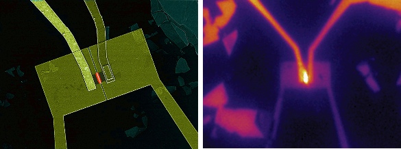
An MIT tungsten diselenide LED under a microscope (left), and in operation (right). (Microscope image, left, by Hugh Churchill and Felice Frankel and device in operation, right, by Britt Baugher and Hugh Churchill, via MIT.[10]
Such tungsten diselenide devices have shown
electroluminescence with a thousand times smaller injection
current and 10 times smaller
linewidth than similar devices made from MoS
2.[5] Says
Jason Ross, a
materials science and engineering graduate student at the University of Washington, and an author of one of the papers,
"These are 10,000 times smaller than the thickness of a human hair, yet the light they emit can be seen by standard measurement equipment... This is a huge leap of miniaturization of technology, and because it's a semiconductor, you can do almost everything with it that is possible with existing, three-dimensional silicon technologies."[11]
One application of such devices would be as
transmitters and
receivers for high speed
optical interconnections on
integrated circuits.[11]
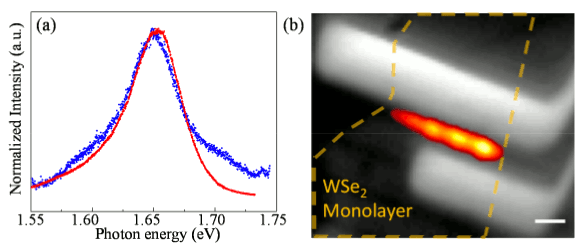
Tungsten diselenide room temperature photoluminescence (blue) and electroluminescence (red), left, along with a photograph of the device with superimposed electroluminescence, right. The orange dashed lines outline the location of the tungsten diselenide layer. The scale bar is 2 μm. (Fig. 3 of ref. 7, via arXiv.[7]
References:
- Extracting two-dimensional materials, University of Washington, YouTube video, March 10, 2014.
- Donald W. Olson, "Graphite," in the 2012 Minerals Yearbook, U.S. Department of the Interior, U.S. Geological Survey, December, 2013 (PDF File).
- M.M. Benameur, B. Radisavljevic, S. Sahoo, H. Berger and A. Kis, "Visibility of dichalcogenide nanolayers," arXiv Preprint Server, June 5, 2010.
- R. Tenne and A. Wold, "Passivation of recombination centers in n‐WSe2 yields high efficiency (>14%) photoelectrochemical cell," Appl. Phys. Lett., vol. 47, no. 7, (October 1, 1985), pp. 707ff.
- Jason S. Ross, Philip Klement, Aaron M. Jones, Nirmal J. Ghimire, Jiaqiang Yan, D. G. Mandrus, Takashi Taniguchi, Kenji Watanabe, Kenji Kitamura, Wang Yao, David H. Cobden and Xiaodong Xu, "Electrically tunable excitonic light-emitting diodes based on monolayer WSe2 p–n junctions," Nature Nanotechnology (March 9, 2014), doi:10.1038/nnano.2014.26.
- Supplementary Information for Ref. 5 (PDF File).
- Jason S. Ross, Philip Klement, Aaron M. Jones, Nirmal J. Ghimire, Jiaqiang Yan, D. G. Mandrus, Takashi Taniguchi, Kenji Watanabe, Kenji Kitamura, Wang Yao, David H. Cobden and Xiaodong Xu, "Electrically tunable excitonic light-emitting diodes based on monolayer WSe2 p–n junctions," arXiv Preprint Server, March 4, 2014.
- Britton W. H. Baugher, Hugh O. H. Churchill, Yafang Yang and Pablo Jarillo-Herrero, "Optoelectronic devices based on electrically tunable p–n diodes in a monolayer dichalcogenide," Nature Nanotechnology (March 9, 2014), doi:10.1038/nnano.2014.25.
- Andreas Pospischil, Marco M. Furchi and Thomas Mueller, "Solar-energy conversion and light emission in an atomic monolayer p–n diode," Nature Nanotechnology (March 9, 2014), doi:10.1038/nnano.2014.14.
- David L. Chandler, "Two-dimensional material shows promise for optoelectronics," MIT Press Release, March 10, 2014.
- Michelle Ma, "Scientists build thinnest-possible LEDs to be stronger, more energy efficient," University of Washington Press Release, March 10, 2014.
Permanent Link to this article
Linked Keywords: Material; nanotechnology; atom; atomic; graphene; carbon; graphite; allotrope of carbon; Scotch Tape; cellophane tape; YouTube video; lubricant; United States Geological Survey; metric ton; United States; hexagonal crystal system; polymorphism; polymorph; boron nitride; chemical element; molybdenum disulfide; molybdenum; Mo; sulfur; S; van der Waals force"; atomic force; arXiv Preprint Serve; tungsten diselenide; tungsten; selenium; photovoltaic; energy conversion efficiency; efficiency; solar simulator; simulated solar radiation; polyiodide; liquid; junction; junction diode; light emitting diode; experiment; Nature Nanotechnology; Massachusetts Institute of Technology; Vienna University of Technology (Vienna, Austria); University of Washington (Seattle, Washington); Justus Liebig University (Giessen, Germany); University of Tennessee (Knoxville, Tennessee); Oak Ridge National Laboratory (Oak Ridge, Tennessee); National Institute for Materials Science (Tsukuba, Japan); University of Hong Kong (Hong Kong, China); research; n-type semiconductor; p-type semiconductor; bias voltage; electrical biasing; metal; electrode; dielectric; hot-carrier injection; electron; electron hole; photodetector; photovoltaic cell; transistor; photosensitivity; ampere; mA; watt; W; external quantum efficiency; absorption of electromagnetic radiation; microscope; Hugh Churchill; Felice Frankel; Britt Baugher; >electroluminescence; electric current; spectral linewidth; Jason Ross; materials science and engineering; postgraduate education; graduate student; human; hair; semiconductor; silicon; fiber-optic communication transmitter; fiber-optic communication receiver; optical interconnect; optical interconnections; integrated circuit; room temperature; photoluminescence; electroluminescence; micrometer; μm; arXiv; YouTube video.