Light Trap
January 7, 2013
Since it's hard to increase the intrinsic
efficiency of
photovoltaic materials, the best method to increase system
energy conversion efficiency is by making certain that all
incident light is available to the
photovoltaic cell. At the least, this means placing
antireflection coatings on the surface to reduce light
reflection. At the best, it involves
microstructuring the surface such that light is "trapped," so it will become completely
absorbed.
In
macro-
optics,
diffraction limits our ability to manipulate light. This limit is descriptively expressed as the limit at which two points separated by a distance
Δx can be resolved. The best-case
diffraction limit, as calculated by
Abbe, is given as
Δx = 0.61λ/n
where
λ is the
wavelength of the light and
n is the
refractive index of the medium, which is typically about 1.5. This translates to a
rule-of-thumb that to resolve features you need a wavelength less than twice the dimension. We can use visible light at a
green wavelength, 550
nm, to resolve features as small as 225 nm, but not very well.
The situation improves when the optical source is very near to the target medium, the so-called
near-field case. None other than
Hans Bethe took time out from his
Manhattan Project responsibilities to
publish a paper on near-field optics,[1] perhaps as a cover for his actual work. The near-field effect was put to good use in 1992 by
Bell Labs scientists as a means for high resolution
scanning optical microscopy (see figure).[2] What we learn from these studies is that light can be manipulated in unusual ways when passed through sub-wavelength
apertures.
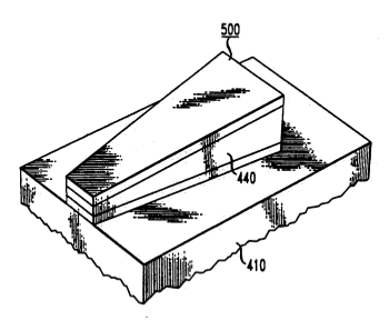
Using a tapered planar waveguide to produce a near-field optical signal.
Figure 11 of US Patent No. 5,272,330, "Near field scanning optical microscope having a tapered waveguide," by Robert E. Betzig and Jay K. Trautman, December 21, 1993.
(Via Google Patents).[3)]
Electrical engineers at
Princeton University have combined a
nanoscale aperture mesh and
plasmons to produce an extremely efficient photovoltaic cell that traps nearly all incident light (see figure). The holes in the mesh are 175 nm in diameter, and this mesh produced a large efficiency enhancement for an
organic photovoltaic cell. Large factors are welcome, since organic photovoltaics, although less expensive, are presently less efficient than their
inorganic competitors.
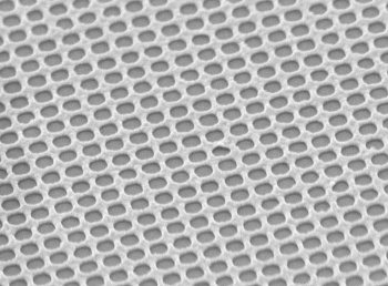
A plasmonic cavity mesh
The holes are 175 nm in diameter, separated by 25 nm, in a 30 nm thick gold film.
(Princeton University Image))
The holes are 175 nm in diameter, separated by 25 nm, in a 30 nm thick
gold film. The efficiency is all the more remarkable, since the mesh shades 40% of the surface area from the incident light. The mesh replaces the typical transparent electrode,
indium-tin oxide, which blocks about 20% of the light.
Stephen Chou, a professor of electrical engineering at Princeton, describes the mesh as "... a
black hole for light."[Princeton] The research team calls the structure a plasmonic cavity with subwavelength hole array, or PlaCSH. The mesh sits atop a transparent 10 nm layer of PEDOT:PSS (
poly(3,4-ethylenedioxythiophene):poly(styrenesulfonate)), an 85 nm layer of photovoltaic
polymer,
P3HT/PCBM, a 5 nm
titanium oxide layer, and a 100 nm
aluminum backing electrode.[5] The layer of PEDOT:PSS, which I wrote about in a
previous article (Transparent and Conductive, June 10, 2011), allows conductance in the hole areas.
In
experiments, these cells have trapped light to an extent that an average light-coupling efficiency of 90% was obtained, with a peak of 96%.[4-5] This excellent light coupling was achieved at all incident angles and all light
polarizations. Unfortunately, because of the low intrinsic efficiency of the photoactive organic layer, these cells achieved just 4.4% power conversion efficiency for a
solar irradiation standard. This was still 52% higher than the equivalent cell without the mesh and an ITO front electrode.[5]
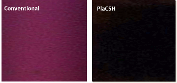
Comparison of the optical absorption of conventional ITO cells and the Princeton PlaCSH photovoltaic cells.
(Princeton University Image))
For scattered light, rather than direct illumination, the mesh structure has an 8% power conversion efficiency, so it would be good for many indoor
energy-harvesting tasks. Another advantage of the mesh is that it has a
sheet resistance of 2.2
ohms per square, which is more than four times lower than that of transparent ITO electrodes. The Princeton team believes that their
wafer-scale process can be adapted for
nano-imprinting of
roll-to-roll material.[5]
Another approach to light trapping is being investigated by scientists at
Duke University, teamed with other scientists from
France and
China, and they've reported their results in a recent issue of
Nature.[6-8] The Duke approach also uses
plasmon resonance, and it's a potentially less expensive process that doesn't require
photolithography. Instead, nanoscale
metal cubes are
randomly scattered on a polymer layer.[7-8] Says team leader,
David R. Smith, an electrical engineering professor at Duke University,
"The nanocubes are literally scattered on the gold film and we can control the properties of the material by varying the geometry of the construct... The absorptivity of large surface areas can now be controlled using this method at scales out of reach of lithography which would otherwise be required to manipulate matter at the nanometer scale."[6]
The photovoltaic device is made by
dip-coating a gold layer with a
dielectric organic layer, and then scattering 74 nm
silver cubes on the surface. In this case, the organic layer was not photovoltaic; instead, it was a combination of
polyallylamine hydrochloride and
polystyrene sulfonate.[7] Incident light excites
electrons in the cubes, and a plasmon resonance is achieved that focuses the light into the dielectric layer.[8]

Artist's conception of nanocubes on a surface.
(Duke University Illustration by Cristian Ciraci).[6)]
Metals alone are
reflective, but the cubes function as optical analogues of
patch antennas.[6-7] The absorptive properties are tailored by the thickness of the film and the size of the nanocubes, and one thing that needs to be optimized in future work is the size uniformity of the cubes.[7-8]
The research was supported by the
Air Force Office of Scientific Research and by the
Army Research Office Multidisciplinary University Research Initiative (MURI).[6]
References:
- H. A. Bethe, "Theory of diffraction by small holes," Phys. Rev., vol. 66, no. 7-8 (October, 1944), pp. 163-182.
- E.Betzig and J.K. Trautman, "Near-field optics: Microscopy, spectroscopy, and surface modification beyond the diffraction limit," Science, vol.257, no. 5067 (July 10, 1992) p.189-195.
- Robert E. Betzig and Jay K. Trautman, "Near field scanning optical microscope having a tapered waveguide," US Patent No. 5,272,330, December 21, 1993.
- John Sullivan, "Tiny structure gives big boost to solar power," Princeton University Press Release, December 5, 2012.
- Stephen Y. Chou and Wei Ding, "Ultrathin, high-efficiency, broad-band, omni-acceptance, organic solar cells enhanced by plasmonic cavity with subwavelength hole array," Optics Express, vol. 21, no. S1 (Jan. 14, 2013), pp. A60-A76.
- Richard Merritt, "Silver Nanocubes Super Light Absorbers," Duke University Press Release, December 6, 2012
- Antoine Moreau, Cristian Ciracì, Jack J. Mock, Ryan T. Hill, Qiang Wang, Benjamin J. Wiley, Ashutosh Chilkoti and David R. Smith, "Controlled-reflectance surfaces with film-coupled colloidal nanoantennas," Nature, vol. 492, no. 7427 (December 6, 2012), pp. 86-89.
- Katharine Sanderson, "Sprinkled nanocubes hold light tight," Nature, December 5, 2012.
Permanent Link to this article
Linked Keywords: Energy conversion efficiency; photovoltaic; material; incident light; photovoltaic cell; antireflection coating; reflection; surface modification; microstructuring; absorption; electromagnetic radiation; macroscopic scale; macro; optics; diffraction; Abbe diffraction limit; Ernst Abbe; wavelength; refractive index; rule-of-thumb; green; nanometer; nm; near-field optics; Hans Bethe; Manhattan Project; scientific literature; Bell Labs; scientist; near-field scanning optical microscope; aperture; planar waveguide; Google Patents; electrical engineer; Princeton University; nanoscopic scale; nanoscale; surface plasmon resonance; plasmon; organic photovoltaic cell; inorganic; gold; indium-tin oxide; Stephen Chou; black hole; PEDOT:PSS; poly(3,4-ethylenedioxythiophene):poly(styrenesulfonate); polymer; P3HT/PCBM; titanium oxide; aluminum; ITO; experiment; polarization; insolation; solar irradiation; energy-harvesting; sheet resistance; ohms per square; wafer-scale; nanoimprint lithography; nano-imprinting; roll-to-roll; Duke University; France; China; Nature; plasmon resonance; photolithography; metal; cube; randomness; random; David R. Smith; dip-coating; dielectric; >organic layer; silver; polyallylamine hydrochloride; polystyrene sulfonate; electron; Cristian Ciraci; patch antenna; Air Force Office of Scientific Research; Army Research Office; Multidisciplinary University Research Initiative; US Patent No. 5,272,330.