Solar Whispers
February 22, 2012
Whispering galleries, usually identified with
acoustics, have recently been popping up in many
optical applications. I described two of these applications in recent articles (
Optical Memory, January 6, 2012 and
Resonant Light Conversion, December 14, 2011). The former application describes a means of storing
data optically in
fiberoptics; and the later describes a means for
efficient harmonic generation of
light.
A recent paper in
Nature Communications describes optical whispering galleries applied to
photovoltaics.[1-3] The research was conducted by a
multidisciplinary team of
Stanford University engineers from the
Department of Materials Science and Engineering, the
Department of Electrical Engineering, and the
Stanford Institute for Materials and Energy Sciences. They used thin,
spherical structures to trap light in whispering gallery modes to absorb nearly every bit of energy from incident
sunlight.
Light-trapping over a wide optical
bandwidth is important to
solar cell efficiency.
Silicon is a widely used photovoltaic material with good efficiency and a large installed based, so any extra efficiency would have a large impact on the amount of electrical
energy harvested. If the light-trapping method lessens the amount of photoactive material, that would lessen deposition time, increase manufacturing throughput, and possibly lead to the development of flexible photovoltaics.[1]
Silicon, in both its
crystalline and
polycrystalline forms, is a very durable material that's been shown to survive long environmental exposure in solar cells.
Nanocrystalline-silicon, however, is a relatively poor light absorber, so a thick layer of the nanocrystalline material is needed in a photovoltaic cell. This problem, the low
optical absorption that leads to the need for thick films, was the motivation for the Stanford research.[2]
The Stanford engineers created hollow microspheres of nanocrystalline-silicon, which they call nanoshells, on the surface of photovoltaic cells (see figure).[2] These nanoshells support the optical whispering gallery
resonant modes that trap light and increase efficiency.[1]
Says lead author of the Nature Communications paper,
Yi Cui,
"The light gets trapped inside the nanoshells. It circulates round and round rather than passing through, and this is very desirable for solar applications."[2]
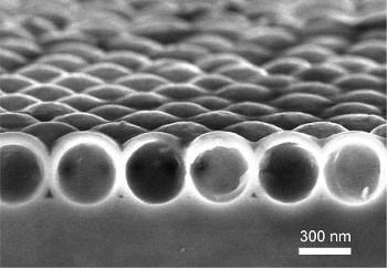
Scanning electron micrograph of a cross section of a layer of hollow nanoshells made of photovoltaic silicon.
(Stanford University Image by Yan Yao))
These nanoshells are fabricated by coating
silica spheres with silicon, and then etching away the silica with
hydrofluoric acid. Silicon does not
react with hydrofluoric acid, so the silicon outer shell remains intact.[2] One further advantage of the nanoshells is that they allow light to enter the silicon from a wide range of
angles. It's estimated that the light in the whispering gallery mode circulates a few times, allowing the energy to be transfered gradually to the underlaying silicon.[2]
The enhanced efficiency was
experimentally confirmed in tests of material with, and without, the nanoshells. The absorption of a single layer of nanoshells, 50
nanometer (nm) thick, was found to be equivalent to a 1000 nm nanocrystalline silicon film without the nanoshells.[1-2] Also, there's no need to stop at just a single layer of nanoshells. The Stanford team achieved a 75% absorption of a portion of the
solar spectrum with a three-layer structure.[2]
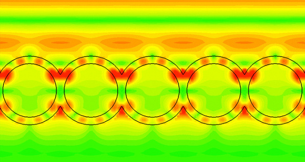
Computer simulation of whispering gallery modes in silicon nanoshells. Light (red/orange coloring), traveling from the top of image to the bottom, creates resonant nodes (red) within the nanoshells. See ref. 3 for an animation. (Stanford University Image by Yan Yao. Used with permission))
Aside from the enhancement in efficiency, there are considerable
manufacturing advantages. A
planar nanocrystalline silicon film of a
micrometer thickness, the required thickness for sufficient optical absorption, takes a few hours to deposit, but the layering of the nanoshells takes just a few minutes, and the resultant photovoltaic cell uses just 5% of the silicon.[2]
Although the process has been proven for silicon, only, it might be applied to other photovoltaic materials, such as
copper indium gallium selenide, which contains the rare and expensive elements
indium and
gallium.
This research was funded as part of Stanford's
Center for Nanostructuring for Efficient Energy Conversion, and by the
U.S. Department of Energy.[2]
References:
- Yan Yao, Jie Yao Vijay Kris Narasimhan, Zhichao Ruan, Chong Xie, Shanhui Fan and Yi Cui, "Broadband light management using low-Q whispering gallery modes in spherical nanoshells," Nature Communications, vol. 3, no. 2 (February 7, 2012), Document No. 664.
- Andrew Myers, "Nanoshell whispering galleries improve thin solar panels," Stanford University Press Release, February 7, 2012.
- Animated electric field distribution in nanoshells at 594 nm, Supplementary Movie at Nature Communications Web Site (2.3 MB)
Permanent Link to this article
Linked Keywords: Whispering gallery; acoustics; optics; optical; data; fiberoptic; energy conversion efficiency; harmonic generation; light; Nature Communications; photovoltaic; multidisciplinary; Stanford University; engineer; Department of Materials Science and Engineering; Department of Electrical Engineering; Stanford Institute for Materials and Energy Sciences; sphere; sunlight; bandwidth; solar cell; silicon; energy; monocrystalline; crystalline; polycrystalline; nanocrystalline-silicon; optical absorption; resonant mode; Yi Cui; Yan Yao; silica; hydrofluoric acid; chemical reaction; angle of incidence; experiment; nanometer; solar spectrum; computer simulation; manufacturing; planar; micrometer; copper indium gallium selenide; indium; gallium; Center for Nanostructuring for Efficient Energy Conversion; U.S. Department of Energy.