A Single-Atom Transistor
February 24, 2012
Moore's Law, the putative trend that the density of
transistors on the highest density
integrated circuits doubles about every two years, has been very good to us. We wouldn't have our magical
smartphones without it, and it's been the acknowledged
roadmap of the
semiconductor industry. One problem with Moore's law is that it predicts single
atom transistors by 2020. As if that isn't difficult enough, what happens after 2020?
In a
previous article (Ohm's Law at the Atomic Scale, January 13, 2012), I reviewed the work by a multinational research team led by
scientists at the
University of New South Wales. This research team demonstrated the scaling of
Ohm's law to a
conductor size just four atoms wide and one atom tall.[1-3] These conductive wires were made by first covering a
silicon surface with
hydrogen, and then using the tip of a
scanning tunneling microscope (STM) to remove the hydrogen in the shape of the wire.
The silicon surface was then doped with
phosphorus atoms by exposure to
phosphine (PH
3). Phosphorus is an
n-type dopant that increases the conductivity of silicon, and in these conductors the dopant density was high, with phosphorus atoms sitting less than a
nanometer from each other.
The phosphorus atoms will only bind to those silicon regions for which the hydrogen has been removed. These doped traces were encased with other silicon atoms to protect them and produce phosphorous-doped silicon wires, just four atoms wide and one atom tall, with a very low
resistivity (~0.3 milliohm-centimeters).
Now, this technology has been used to produce a transistor based on a single phosphorus atom.[4-11] The use of a single atom of
phosphorus-31 (
31P) opens the possibility that such devices could form the basis of a
quantum computer. An isolated dopant atom has a long
coherence time of
quantum states.[4]
In theory, the two possible
nuclear spin states of
31P could serve as a "
qbit," a
quantum information state that represents many values, not just a "1" or "0." [7-8] The trick to quantum computation is that there can be interaction between qbits for
computation only if the location of the qbits is precisely known. Placing single atoms precisely in a
crystal lattice solves this problem.[10]
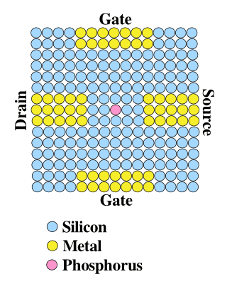
Layout of the single atom transistor. The phosphorus atom sits between the metal gate, source and drain electrodes. There are actually more than a hundred rows of silicon atoms between the gate electrodes and the phosphorus atom, and tens of rows between the drain and source electrodes and the phosphorus atom.
Illustration by the author, rendered in Inkscape. [5]
The transistor layout, as shown in the above figure, consists of the phosphorus atom surrounded by electrodes.[5] The
source and
drain metalizations are separated by a 108
nanometer gap, while the
gate electrodes have a 20 nanometer gap between them. [10]
The phosphorus atom can be placed into three possible
charge states; namely, a zero-
electron state, a one-electron state, and a two-electron state. Not surprisingly because of its
quantum mechanical nature, this device will only operate at very low
temperatures (<1
kelvin). It is only at these temperatures that the electrons are confined to their proper channels.[9-10]
This is not the first single atom transistor. A single atom transistor was first demonstrated in 2002, but
reproducibility for single atom devices has been a problem. Generally, many devices were needed to be made to find a single working device.[6-7] The STM fabrication method, although laborious, routinely produces working devices.[6]
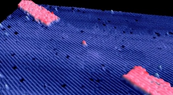
Scanning tunneling micrograph of a portion of a single-atom transistor.
(Screen capture from a YouTube video).[11)]
This device demonstrates the fundamental limit of transistor technology. The industry appears to be at a
tipping point between the old, top-down approach of
photolithography, and the newer, bottom-up approaches that build electronic devices atom-by-atom. What's needed now are improved tools that can facilitate the atom-by-atom approach.
References:
- B. Weber, S. Mahapatra, H. Ryu, S. Lee, A. Fuhrer, T. C. G. Reusch, D. L. Thompson, W. C. T. Lee, G. Klimeck, L. C. L. Hollenberg and M. Y. Simmons, "Ohm's Law Survives to the Atomic Scale," Science, vol. 335, no. 6064 (January 6, 2012), pp. 64-67.
- David K. Ferry, "Perspective-Applied Physics, Ohm's Law in a Quantum World," Science, vol. 335, no. 6064 (January 6, 2012), pp. 45-46.
- Univeristy of New South Wales video about atom-sized conductor.
- Gabriel P. Lansbergen, "Nanoelectronics: Transistors arrive at the atomic limit," Nature Nanotechnology, Document Number 2012.23, February 19, 2012.
- Martin Fuechsle, Jill A. Miwa, Suddhasatta Mahapatra, Hoon Ryu, Sunhee Lee, Oliver Warschkow, Lloyd C. L. Hollenberg, Gerhard Klimeck and Michelle Y. Simmons, "A single-atom transistor," Nature Nanotechnology, Document Number 2012.21, February 19, 2012.
- Bob Beale, "Single-atom transistor is 'perfect'," University of New South Wales Press Release, February 20, 2012.
- John Markoff, "Physicists Create a Working Transistor From a Single Atom," The New York Times, February 19, 2012.
- Alex Knapp, "Scientists Create A One-Atom Transistor," Forbes, February 12, 2012.
- Richard Chirgwin, "Tiny transistor stays where it's put," Register (UK), February 19, 2012.
- Melissae Fellet, "Single atom transistor gets precise position on chip," New Scientist, February 19, 2012.
- YouTube video on the single atom transistor by the University of New South Wales
Permanent Link to this article
Linked Keywords: Moore's Law; transistors; integrated circuit; smartphone; technology roadmap; semiconductor industry; atom; scientist; University of New South Wales; Ohm's law; electrical conductor; silicon; hydrogen; scanning tunneling microscope; phosphorus; phosphine; n-type dopant; nanometer; resistivity; phosphorus-31; quantum computer; coherence time; quantum state; nuclear spin; qbit; quantum information state; computation; crystal lattice; gate; drain; source; Inkscape; metalization; charge; electron; quantum mechanics; temperature; kelvin; reproducibility; scanning tunneling micrograph; YouTube video; tipping point; photolithography.