Welding Nanowires
February 10, 2012
One area in which I worked extensively was
high temperature sensors. Portions of
gas turbine engines are very hot, but these quite complicated machines still need to be monitored for safety, and to enhance performance.
A common technique is to infer the operation of a hot section by monitoring something in a cooler section, such as gas
pressure and
flow. These are indirect measurements that rely on
computer models, so the data they provide can lag the actual values by a few seconds, and they're not as satisfying as having a real sensor in the right place.
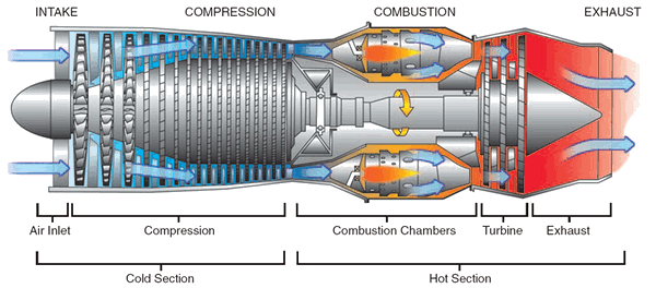
Basic components of a gas turbine engine. Federal Aviation Administration diagram, via Wikimedia Commons)
One of my
position sensors[1] operated at more than 500°
C, and the biggest problem that I had in its development was making
electrical connections of the various components to withstand those temperatures.
Common solders work to about 300°C, but above that range you need to
weld, and the usual option is
electric resistance welding.
Resistance welders are used for such bonding tasks as assembling
automobiles, but they are often used in assembly of small electric and
electronic devices such as the filaments in (
soon-to-be-outlawed)
incandescent light bulbs. The resistance welding principle is very simple.
A
current pulse is sent through
copper electrodes that press from opposite sides of the
metal components to be welded.[2] Because of
contact resistance, the heating power (
I2R) is concentrated at the junction between the components. Selecting the proper current and pulse time allows controlled
melting of the metals into each other to make a junction.
My application was bonding tiny
wires of just
a few thousandths of an inch in diameter, but a team of
materials scientists at
Stanford University and their collaborators have achieved a welding record by using a novel process to weld wires more than three
orders of magnitude smaller. The process uses
light-induced
plasmons to weld
silver nanowires in
mesh networks used as
transparent conductors.[3-4]
Nanowire meshes are being researched as a means to make the transparent conductors used in
displays and
photovoltaic cells and replace
Indium-tin oxide (ITO, typical composition 90%
In2O3 and 10%
SnO2 by weight) for these applications.
Indium is becoming scarce and expensive. The average price of indium in 2010 was about $560/
kg.[5]
I reviewed a
chemical approach to bonding silver nanowires in a
recent article (Silver Nanowire Transparent Electrodes, December 19, 2011). A
UCLA research team used a technique that brought nanowires into close contact. The conductive polymer,
PEDOT:PSS (poly(3,4-ethylenedioxythiophene) poly(styrenesulfonate)) coating was then used to establish the connections.[6-7]
The Stanford approach is an actual welding process. It's no wonder that silver is used as the wire material. Not only is silver highly conductive, but its
surface plasmons are at
ultraviolet wavelengths (3.9
eV). Light from a
laser excites these surface plasmons, which are an
oscillation of
electrons at the optical
frequency, in the silver wires. This electron excitation is enough to melt the silver in the regions where wires contact each other (see photograph).
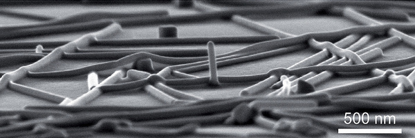
A welded silver nanowire mesh. The top nanowires direct the plasmons into the bottom wires to create enough heat to weld the wires together. (Stanford University image by Mark Brongersma, used with permission.)
The plasmons are concentrated at the gaps between the wires, so the heating is localized to these areas. The process is nicely self-limiting, since the welding eliminates the gaps and terminates the heating. This allows formation of silver meshes on inexpensive, flexible, low temperature materials. [3-4] As a demonstration, the Stanford team made a conductive mesh on a sheet of
Saran wrap. They were able to crumple the sheet and still maintain conductivity.[4]
This research was supported by the
Center for Advanced Molecular Photovoltaics at Stanford University, which is funded by the
King Abdullah University of Science and Technology.[4]
References:
- Devlin M. Gualtieri, "Temperature compensated resonant transmission line sensor," US Patent No. 7,373,272, May 13, 2008.
- A lesser used technique, which is good for welding wires to flat conductors, has closely spaced electrodes that press the wire against the conductor. The current passes through both contacts, creating two welds at the same time.
- Erik C. Garnett, Wenshan Cai, Judy J. Cha, Fakhruddin Mahmood, Stephen T. Connor, M. Greyson Christoforo, Yi Cui, Michael D. McGehee and Mark L. Brongersma, "Self-limited plasmonic welding of silver nanowire junctions," Nature Materials, Document No. 3238, February 5, 2012.
- Andrew Myers, "Stanford engineers weld nanowires with light," Stanford University Press Release, February 6, 2012.
- US Geological Survey, Indium - USGS Mineral Resources Program, Mineral Commodity Summaries, 2011.
- Jennifer Marcus, "UCLA team develops highly efficient method for creating flexible, transparent electrodes," UCLA Press Release, November 21, 2011.
- Rui Zhu, Choong-Heui Chung, Kitty C. Cha, Wenbing Yang, Yue Bing Zheng, Huanping Zhou, Tze-Bin Song, Chun-Chao Chen, Paul S. Weiss, Gang Li and Yang Yang, "Fused Silver Nanowires with Metal Oxide Nanoparticles and Organic Polymers for Highly Transparent Conductors," ACS Nano (DOI: 10.1021/nn203576v), October 28, 2011.
Permanent Link to this article
Linked Keywords: High temperature; sensors; gas turbine engine; pressure; flow; computer model; Federal Aviation Administration; Wikimedia Commons; position sensor; Celsius; C; electrical connection; solder; ; weld; electric resistance welding; automobile; electronic device; phase-out of incandescent light bulbs; soon-to-be-outlawed; incandescent light bulb; current; pulse; copper; electrode; metal; contact resistance; I2R; melting point; melting; wire; AWG wire size; materials scientist; Stanford University; orders of magnitude; light; plasmon; silver; nanowire; mesh network; transparent; conductor; display; photovoltaic cell; indium-tin oxide; In2O3; SnO2; indium; kilogram; kg; chemical reaction; University of California, Los Angeles; UCLA; PEDOT:PSS; ultraviolet wavelength; electronvolt; eV; laser; surface plasmon; oscillation; electron; frequency; Mark Brongersma; Saran wrap; Center for Advanced Molecular Photovoltaics; King Abdullah University of Science and Technology; US Patent No. 7,373,272.